
DFMA for electronics manufacturing
DFMA – Design for Manufacturing and Assembly
What is DFMA for electronics manufacturers?
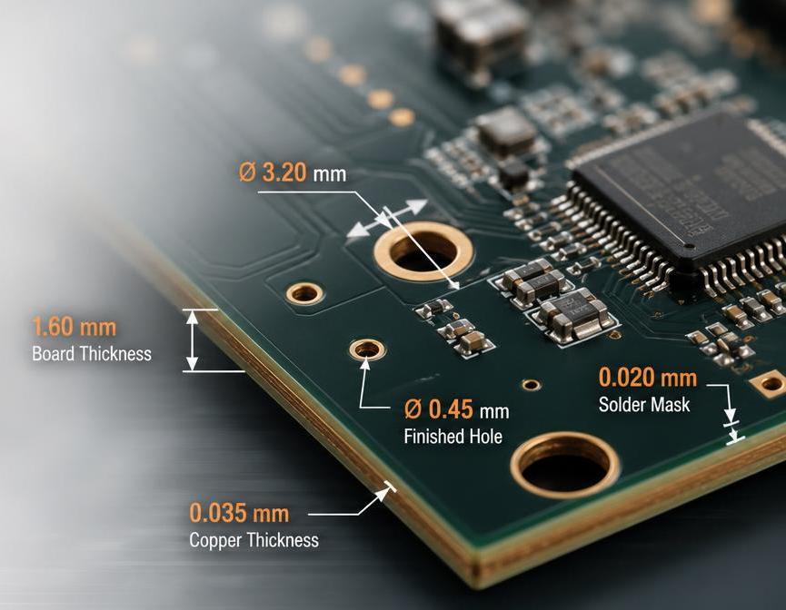
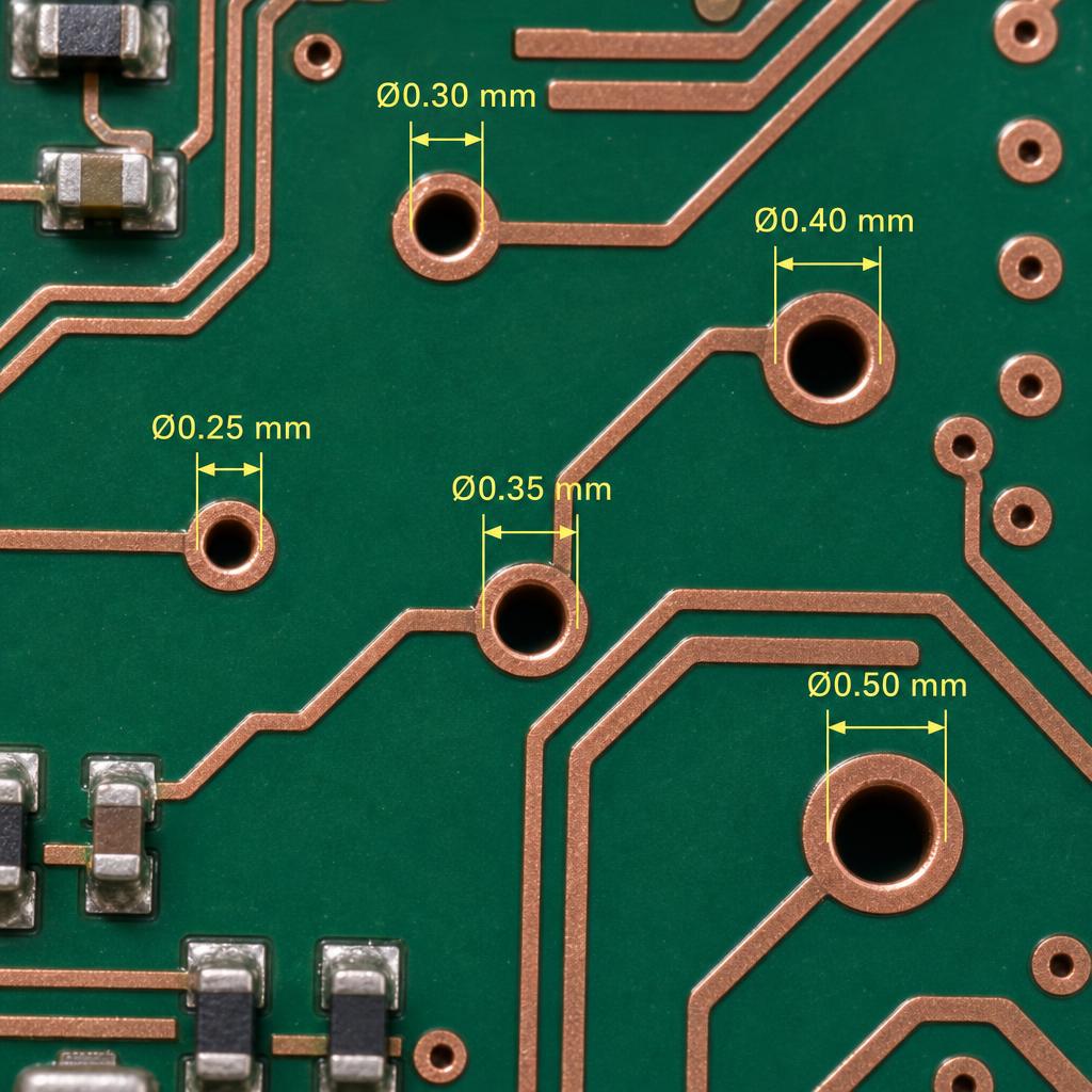
This involves examining, amongst other things, printed circuit board layouts, drill holes, components, solder joints and assembly feasibility, in order to identify manufacturing problems at an early stage and to avoid additional costs and optimisation loops as far as possible.
The aim of DFMA is to
- increase manufacturing efficiency
- reduce sources of error
- lower manufacturing costs
- ensure timely market entry
Why use automated DFMA in the EMS industry?
- Optimal time-to-market combined with reliable quality are more important than ever for electronics customers today.
- The earlier a problem can be identified in the time-to-market process, the lower the additional costs and the less time is lost.
Manual layout checks are a time-consuming process during which important details can easily be overlooked.
- Quickly align customer requirements with your PCB manufacturer’s design guidelines
- Early consultation with customers regarding manufacturing tolerances and risks
- Early detection of layout errors to ensure on-time market launch
With automated DFMA, leave the data analysis to the algorithms and give your experts more time to discuss solutions with your customers.
The EMS business is a business built on trust and thrives on consultancy and early fault detection. That is why DFMA can help you strengthen your customers’ trust through early fault prevention.
DFMA – An Overview of Manufacturability
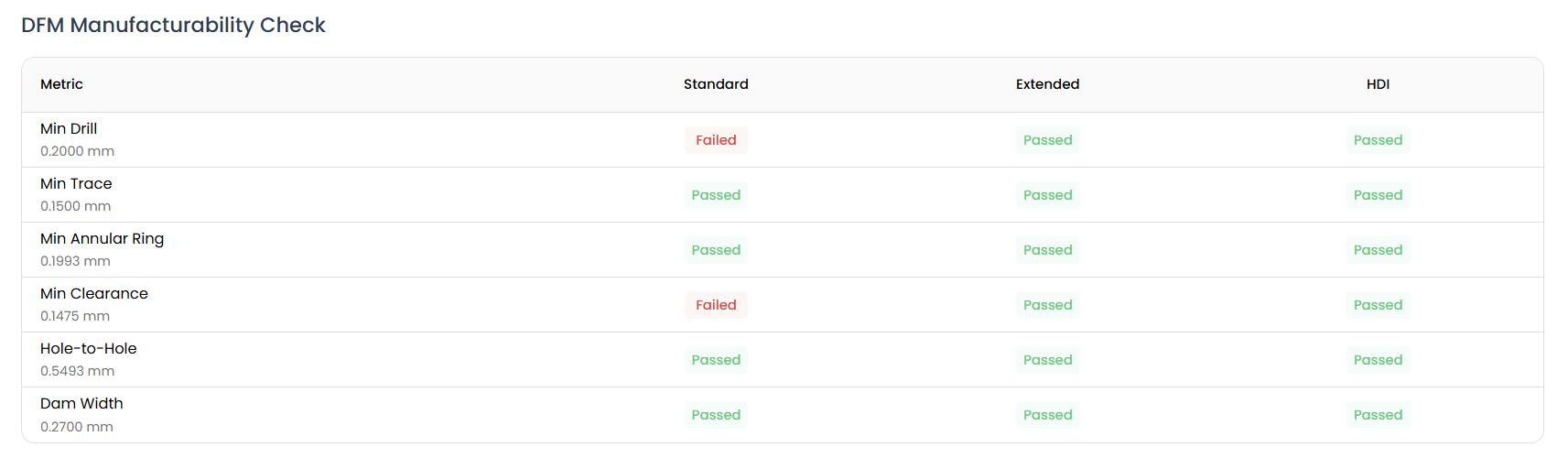
In a matter of moments, you can identify manufacturability risks or problems and provide your customers with targeted support in optimising their layouts, thereby saving them time and avoiding additional hardware costs.
DFMA – Pad classification
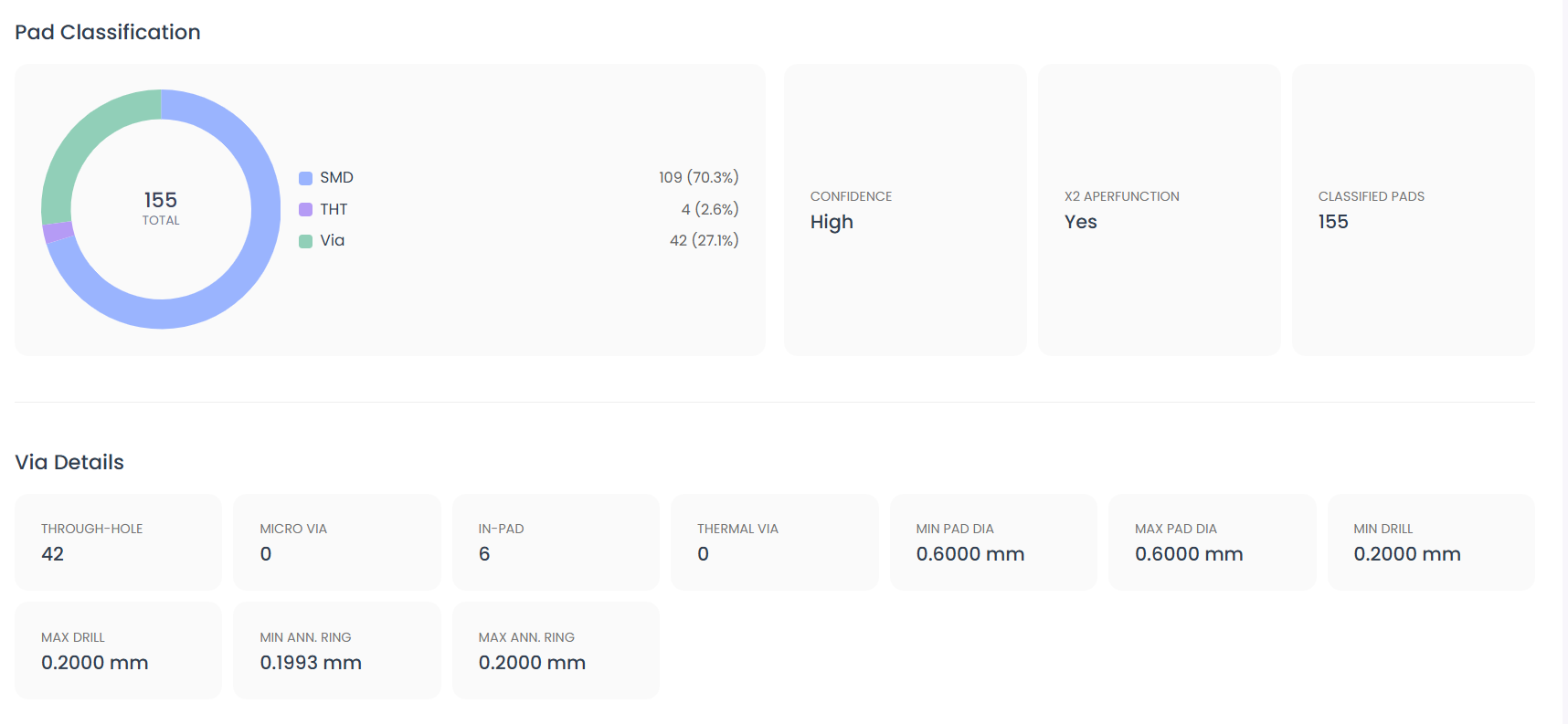
This enables critical pad geometries to be systematically identified and targeted optimisation recommendations to be provided to your customers to ensure a stable, reproducible soldering process.
DFMA – Clearances
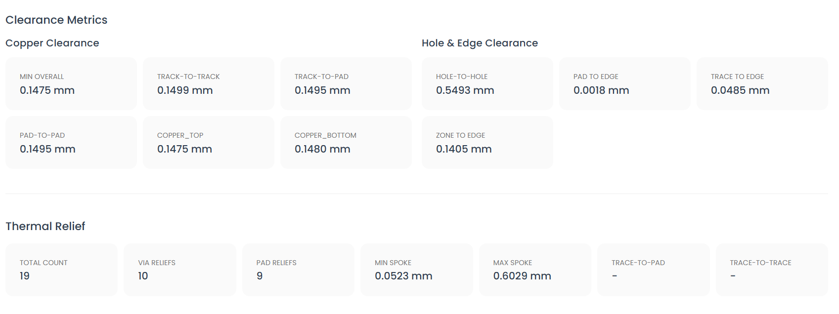
By identifying clearances that are too small in the PCB layout at an early stage and reporting them back to your customers, you create added value that saves both development and testing time, as well as the costs associated with further hardware iterations.